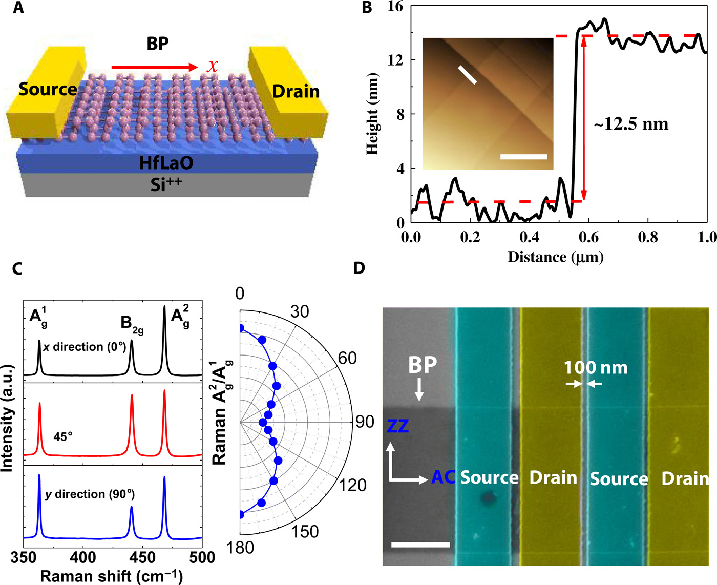
Figure 1 | The characterization of the device structure.(a) Schematic of a back-gated BP on an HfLaO substrate with top Ni/Au source and drain electrodes. (b) The BP flake with a measured thickness of 12.5 nm by AFM. Inset of (b), AFM image of the few-layer BP devices. The scale bar is 2 µm. (c) Polarization-resolved Raman spectrum of the BP flake. The left image shows three spectra obtained from an individual flake in different orientations. The right image shows the orientation dependent A2g/A1g peak intensities. (d) A representative false-colored SEM image of the BP transistors. AC and ZZ stands for the armchair and zigzag directions, respectively. The scale bar is 1 µm.
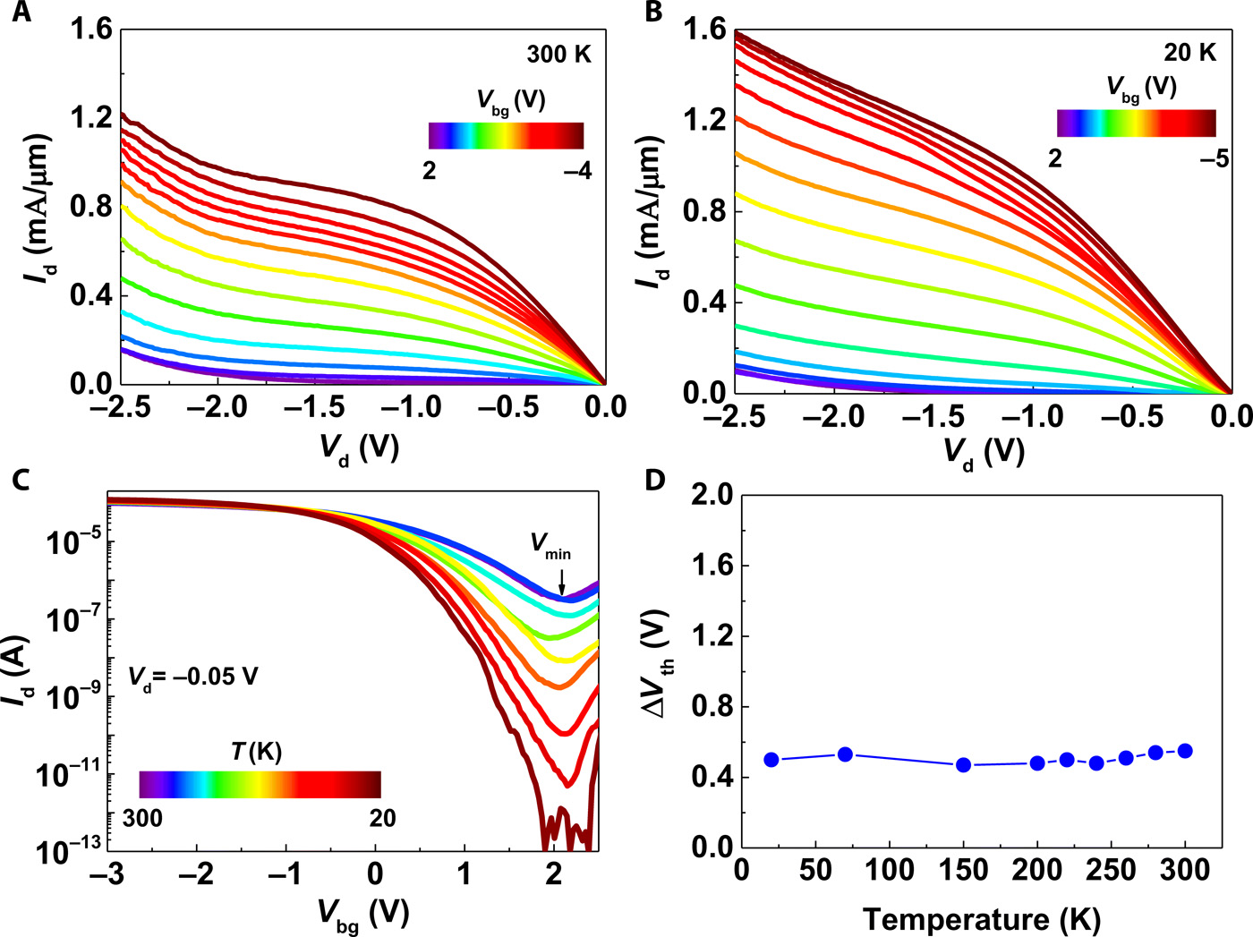
Figure 2 |Transport properties of BP transistor at low temperature.(a)Output characteristics of the BP device with a channel length of 100 nm at 300 K. (b) Output characteristics of the same device at 20 K.(c) Transfer characteristics of the 100-nm device for BP on HfLaO at different temperatures. (d) Hysteresis values of the 100-nm device for BP on HfLaO as a function of temperature.

Figure 3 | Saturation velocity of BP FETs.(a) Drift velocity as afunction of transverse electric field in the channel for the 100 nm channel-length BP device at 300 and 20 K. Scatters are experimental data; solid lines are fits to and extrapolation from eq 4. (b) Extracted saturation velocity versus temperature at various hole densities. (c) Comparison of hole saturation velocity as a function of bandgap for different materials at room temperature.

Figure 4 | Ballistic simulation of BP FETs.Comparison of the (lines) MVS model fit and (symbols) measured data for the Id-Vd characteristics in Fig. 2. (a) 300 K. (b) 20 K. (c) Benchmark of ballistic efficiency in this work with Si planar MOSFET.
(Science Advances 21 Jun 2019: Vol. 5, no. 6, eaau3194, DOI: 10.1126/sciadv.aau3194)
Background
So far, most studies focus on BP devices with thick thermally oxidized SiO2 as back-gated dielectrics, which typically yields unsatisfactory electronic properties. Therefore, the integration of high-quality dielectrics with BP is an important scientific and technological challenge. Another unique property of BP is its anisotropic properties due to the highly asymmetric effective mass, which enables the utilization of the lower effective-carrier-mass transport along the armchair direction for better performance transistors. Moreover, saturation velocity plays a significant role in determining device performance especially in short channel transistors, and hole saturation velocity in conventional semiconductors and two dimensional transition metal dichalcogenides are typically much lower than that of electron. High hole saturation velocity in BP 2D semiconductors is vital for realizing high performance optoelectronics and electronics. However, very few studies of saturation velocity in short-channel BP FETs have been reported to date in spite of the importance in fundamental and practical application.
What we discover?
In this work, we introduce an ultra-thin high-k HfLaO as the back gate dielectric to increase the electrostatic doping and improve the interface quality. The equivalent oxide thickness (EOT) of the HfLaO dielectric in this work is around 2.7nm. The application of -4 V back gate (Vbg) voltage induces a much higher carrier density of 2.1×1013cm-2 than those using the typical SiO2, owing to the combination of high-kproperty and excellent dielectric breakdown property. The high carrier density results in an increase of electrostatic doping of BP underneath the metal contact with a lower Schottky barrier, which facilitates the hole injections from the source metal into the channel which results in a reduced Rc. The minimal Rc of 0.7 kΩ·µm and the maximum drain current of 1.2 mA/μm for the 100 nm channel length BP device are obtained at room temperature. Furthermore, the drain current increases to around 1.6 mA/μm at 20 K when ballistic transport is effectively realized. Furthermore, we extract a saturation velocity of 1.5×107cm/s at room temperature, which outperforms silicon and other layered 2D semiconductors and reaches the highest value for hole saturation velocity.
Why is this important?
We have demonstrated, for the first time,ballistic transport of few-layer BP FETs with HfLaO dielectrics as the back-gate substrateand performed theoretical modeling to gain insight into theballistictransport mechanisms.A record high on-current density of 1.2 mA/μm at 300 K and 1.6 mA/μm at 20 K is achieved, which are mainly attributed to the high quality HfLaO films, excellent interface between HfLaO and BP, as well as the ultra-high electrostatic doping to form low Rc. A record high field hole saturation velocity of BP FETs of 1.5×107cm/s at 300 K can be obtained. The ballistic transport behavior of BP short channel device is assessed by the MVS model, demonstrating a ballistic efficiency of 79.4% at 20 K.All these results make few-layer BP a very promisingcandidate material for future applications in high-speed electronics andoptoelectronics.
Who did the research?
Xuefei Li1#,Zhuoqing Yu2#, Xiong Xiong1, Tiaoyang Li1, Tingting Gao1,Runsheng Wang2, Ru Huang,2and Yanqing Wu1*
1Wuhan National High Magnetic Field Center and School of Optical and Electronic Information, Huazhong University of Science and Technology, Wuhan 430074, China
2Institute of Microelectronics, Peking University, Beijing 100871
Funding
This work was supported by the National Natural ScienceFoundation of China (grant nos. 61574066, 61874162, and 61522402), the Strategic PriorityResearch Program of Chinese Academy of Sciences under grant no. XDB30000000 and,in part, by the Fundamental Research Funds for the Central Universities under grant 2018KFYYXJJ069 and 2019kfyXKJC014.

