
Fig. 1: Material characterization of thin ITO film.
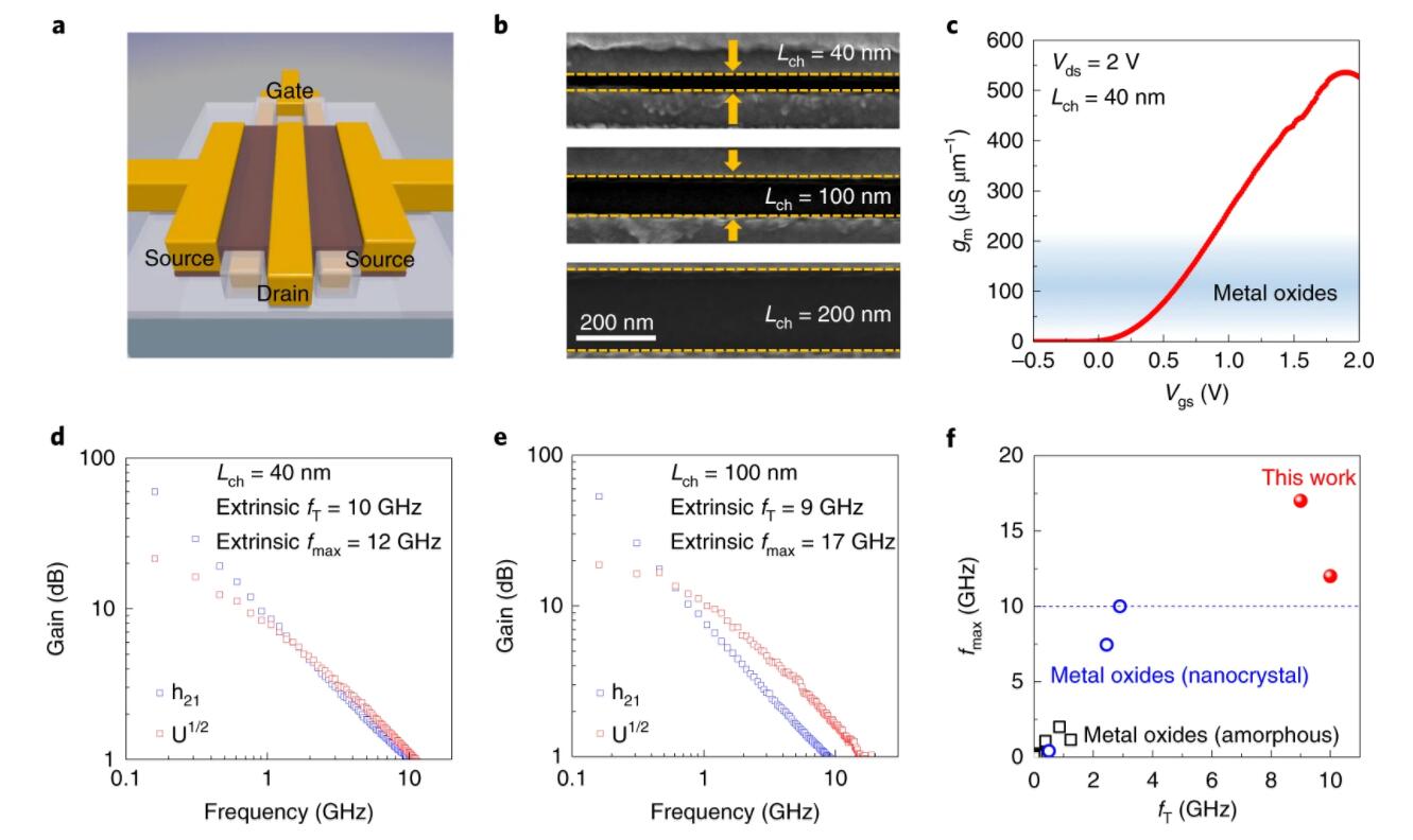
Fig. 2: High performance of RF transistors based on ITO.
(Nature Material 18, 2019, DOI:https://doi.org/10.1038/s41563-019-0455-8)
Background
In recent years, with increasing demand of wearable applications and portable devices, ultra-low-power electronics have been a research hotspot. Devices based on new materials face many challenges such as large-area synthesis, performances of ultra-short channel device, compatibilities between technology and existing planar transistor fabrication technology.
What we discover?
Indium tin oxide, also known as ITO, is a wide-bandgap semiconductor with high mobility and low dielectric constant, providing prospects for future scaling below the 5-nm regime for advanced low-power electronics. It is widely used as transparent conductive electrodes in display and energy fields due to high conductivity, but its metal-like properties prevent devices from turning off, limiting its applications in the active region of transistors.By precisely controlling the sputtering atmosphere and interfacial doping in the deposition process of ITO, we obtained a 4-nm ITO film with a smooth surface and extremely high consistency, and realized fully depletion through quantum constraint effect. By using high k material of La-doped HfO2(HfLaO) as the gate oxide, the equivalent physical thickness (EOT) of 0.8 nm was obtained, and excellent interface characteristics were achieved. Besides, the ITO transistors remained excellent device performance when the channel lengths were decreased from 30 μm to 40 nm, showing a switching ratio larger than 9 decades and a subthreshold slope less than 70 mV/dec.
Why is this important?
In this work, the excellent immunity of short-channel-effect for 40-nm ITO device was mainly attributed to the ultra-thin device body and perfect interface quality. The comprehensive performances of on-state current and switch ratio for 40-nm ITO device were much better than that of previous devices based on two-dimensional materials and other metal-oxides. At the same time, the logic inverter constructed by ITO transistors achieved a record high gain of 178 at 0.5 V. Besides, the extrinsic cut-off frequency fT, and maximum oscillation frequency fmaxof the 40-nm-long ITO device were both beyond 10 GHz, which were also much higher than the previous metal oxides and two-dimensional materials. These results provide prospects for further research on advanced low-power electronics when the characteristic length is reduced to 5 nm.
Who did the research?
Shengman Li1, Mengchuan Tian1, Qingguo Gao1, Mengfei Wang1, Tiaoyang Li1, Qianlan Hu1, Xuefei Li1and Yanqing Wu1,2*
1Wuhan National High Magnetic Field Center and School of Optical and Electronic Information, Huazhong University of Science and Technology, Wuhan, China.
2Institute of Microelectronics and Key Laboratory of Microelectronic Devices and Circuits, Peking University, Beijing, China.
Acknowledgements
This work was funded by the National Natural Science Foundation of China and various projects of our university, and strongly supported by the Wuhan National High Magnetic Field Center, as well as the technical support of the Center of Micro-fabrication and Characterization of Wuhan National Laboratory for Optoelectronics, and Huazhong University of Science and Technology Analytical and Testing Center.

