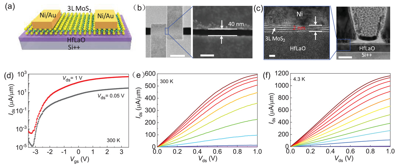
Fig1. (a) Schematic of bottom-gated trilayer MoS2 FETs with Ni/Au contacts. (b) SEM images of the trilayer MoS2 device. The scale bar is 2 µm. The contact bars with a length of 2 μm were defined by e-beam lithography. The right panel shows the zoom-in image of the trilayer MoS2 transistor with a channel length of 40 nm. The scale bar is 100 nm. (c) Cross-sectional high-resolution TEM images of the 40 nm MoS2 FET region. The scale bar is 20 nm. The left panel shows the zoom-in image of the trilayer MoS2 contact region. The scale bar is 2 nm. (d) Transfer characteristics of the 40 nm MoS2 transistor at room temperature. (e) Output characteristics of the 40 nm MoS2 transistor at room temperature. (f) Output characteristics of the same device at 4.3 K.
Background
In the past few years, two-dimensional (2D) molybdenum disulfide (MoS2) hasattracted tremendous research attentiondue to its atomically thin layered structure and high carrier mobility.These features make MoS2 especially interesting as a promising candidate for many applications. Importantly, it is believed to beimmune against short-channel effects because of the ultrathin body channel.However, the overall performance of short-channel MoS2 FETs based on CVD monolayer MoS2 in previous studies is still substantially lower than those of conventional Si FETs at the same channel length. One of the main limiting factors is the physical damage of the monolayer crystal during metal deposition, leading to a substantial contact resistance Rc, which becomes the bottleneck for device performance, especially in short channel devices. Moreover, saturation velocity vsat, instead of mobility, is critical to determine the on-state current for short-channel transistors and is still largely lacking. It also limits the intrinsic frequency of a transistor based on fT∼vsat/(2πLch).Here, we successfully demonstrate the epitaxy growth of trilayer MoS2 single crystals on soda-lime glass substrates and high-performance short channel trilayer MoS2 FETs.
What is discovered?
we have grown large domain and high mobility trilayer MoS2 crystalson soda-lime glass substrates by a scalable CVD approach. Spectroscopic characterizations reveal a weak interface interaction between MoS2 and soda-lime glass. Clear and sharp atomic-resolution STEM imaging determines the ABB stacking sequences in CVD-grown trilayer MoS2. The short-channel MoS2 transistors with ultrathin HfLaO dielectrics exhibit a high drain current (589 μA/μm atVds= 1 V) as well as record-high saturation velocity (4.2´106 cm/s) at room temperature, which increases further at 4.3 K. The excellent electrical properties of the trilayer channelenablereduced surface scattering and lower contact resistance compared with the monolayer channel counterpart, making it a promising 2D material for future electronics applications.
What is important?
Trilayer MoS2, with high mobility and higher density of states, has attracted great interest recently, withextensive studies oncontrollable high-quality growth methods. Although considerable efforts have been devoted to growing trilayer MoS2 films on SiO2 or sapphire substrates, they commonly suffer from extensive domain/grain boundaries,substrate-induced defects, and small domain size, as well as inferior electrical properties compared with exfoliated ones. The growth of trilayer MoS2 on soda-lime glass substrates is stillunderdeveloped.
Why did we need WHMFC?
Micro/Nano Fabrication Platform provides sufficient cleanrooms of high level cleanness, in which micro-nano scale materials and devices may be fabricated and tested. High end facilities includes: vacuum sputtering coating system, light lithography system、etching system, etc., which will support for high quality fabrication and characterization of complex quantum electric circuits.
Who did the research?
Xuefei Li1,*, Zhenfeng Zhang1, Tingting Gao1, Xinhang Shi1, Chengru Gu1, and Yanqing Wu1,2,*
1Wuhan National High Magnetic Field Center and School of Electrical and Electronic Engineering, Huazhong University of Science and Technology, Wuhan 430074, China
2School of Integrated Circuits, Peking University, Beijing 100871
*Corresponding authors: xfli@hust.edu.cn; yqwu@pku.edu.cn
Link
https://onlinelibrary.wiley.com/doi/10.1002/adfm.202208091

