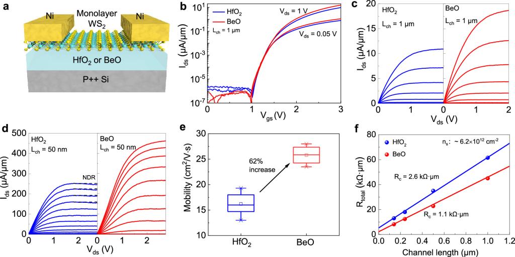
Figure 1. a)Schematic of the monolayer WS2 back-gate FET fabricated in this work. The gate dielectric is 10 nm HfO2 or 8 nm BeO. The S/D contact metal is Ni (20 nm)/Au (40 nm).b)Ids-Vgs transfer curves of monolayer WS2 transistors with 10 nm HfO2 and 8 nm BeO dielectrics. Both the channel length and channel width are 1 µm.c) The corresponding Ids-Vds output characteristics of the monolayer WS2 transistors.Vgs changes from 0 to 3 V.d) The Ids-Vds output characteristics of the monolayer WS2 transistors with a channel length of 50 nm.Vgs changes from -0.5 to 4 V. e) Statistical distribution of field-effect mobility of water-assisted transferred monolayer WS2 on HfO2 or BeO dielectrics. f) TLM resistances of monolayer WS2 transistors with HfO2 and BeO dielectrics.
Background
Two-dimensional (2D) transition-metal chalcogenides (TMDs) have attracted intensive attention in recent years, owing to their atomically thin body nature,which enables further scaling for next-generation electronic devices. Recently,tungsten disulfide (WS2) has attracted increasing research interest due to its larger band-gap (~ 2 eV), smaller effective mass, and higher injection velocity among the TMDs family, all of which are vital for low-power and high-performance devices. To explore the full potential of WS2 transistors, it is of great importance to study high-field transport on short-channel devices, where heat dissipation plays a critical role, especially at high current densities. Furthermore, a recent theoretical study predicts an even lower thermal conductivity in WS2 compared with the commonly studied MoS2, which requires further optimizations in thermal management to preventdevice performance degradation and failure.However,mostmonolayer WS2 devices reportedthusfar typicallyemploythermally oxidized 300-nm-thick (or 100-nm-thick) SiO2 as the back-gate dielectric, resulting inlow on-state current and transconductance (gm), which is not only far from the desired operation region for studying power dissipation but also unsuitable for the performance boost.In this work, we demonstrate high-performance n-type monolayer CVD WS2 FETs with a high-quality BeO dielectric.
What is discovered?
We have demonstrated high-performance monolayer CVD WS2 transistors on a high-thermal-conductivity BeO dielectric for the first time, which effectively facilitates heat dissipation and suppresses the self-heating effect. Notably, the 50-nm short channel device shows a high Ion/Ioff ratio of 1.8×10⁸, gm of 150 μS/μm, and Ion of 325 μA/μm at Vds= 1 V, which are record values among all reported monolayer CVD WS2 transistors. The promising results of this work provide a scalable and reliable method to achieve high-performance TMDs transistors for future electronics.
What is important?
Although hafnium dioxide (HfO2) is the most widely used high-kdielectric, the thermal conductivity is quite small (~23 W/K×m). Compared with HfO2, beryllium oxide (BeO) hasamuch higher thermal conductivity (~330 W/K×m), which is beneficialfor alleviatingthe self-heating effect andimprovingdevice performance and reliability. On the other hand, it also exhibits a larger bandgap (Eg = 10.6 eV) with a decent dielectric constant (~ 8.7), which helps reduce the gateleakage current at higher electric fields. Meanwhile, it can also be grown by atomic layer deposition (ALD) with precise thickness control on a wafer scale.Previously, BeO was used as a gate dielectric in III-V and Si field-effect transistors (FETs), exhibiting excellent interface quality. Nevertheless, the advantageous thermal conductivity of BeO in atomic thin TMDs-based transistors has yet to be explored.
Why did we need WHMFC?
Micro/Nano Fabrication Platform provides sufficient cleanrooms of high level cleanness, in which micro-nano scale materials and devices may be fabricated and tested. High end facilities includes: vacuum sputtering coating system, light lithography system、etching system, etc., which will support for high quality fabrication and characterization of complex quantum electric circuits.
Who did the research?
Xinhang Shi1, Xuefei Li1,*, Qi Guo1, Han Gao1, Min Zeng1, Yibo Han1, Shiwei Yan1, and Yanqing Wu1,2,*
1Wuhan National High Magnetic Field Center and School of Optical and Electronic Information, Huazhong University of Science and Technology, Wuhan 430074, China
2School of Integrated Circuits, Peking University, Beijing 100871, China
*Authors to whom correspondence should be addressed: xfli@hust.edu.cn; yqwu@pku.edu.cn
Link
https://pubs.acs.org/doi/10.1021/acs.nanolett.2c02901?ref=PDF
